
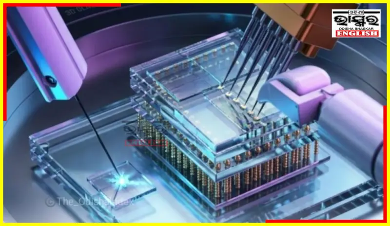

Bhubaneswar: Odisha marked a historic leap in India's technology journey on Sunday as the foundation stone was laid for the country's first advanced 3D semiconductor packaging unit at Info Valley.
The project, spearheaded by US-based 3D Glass Solutions through its Indian arm, positions the state at the forefront of next-generation electronics manufacturing and strengthens the nation's Atmanirbhar Bharat vision.
Chief Minister Mohan Charan Majhi hailed the initiative as a "milestone moment," noting it is the first time such cutting-edge 3D glass semiconductor technology is being established in India. He emphasized Odisha's growing appeal as a global tech investment hub, with interest already flowing from giants like Intel, Lockheed Martin, and Applied Materials.
The facility, backed by nearly Rs 2,000 crore in investment, will produce around 70,000 glass panels annually, 50 million assembled units, and 13,000 advanced 3D heterogeneous integration modules. Its applications span critical sectors including Artificial Intelligence, defence electronics, telecommunications, and high-performance computing, making it a strategic asset for India's technological self-reliance.
Union Minister Ashwini Vaishnaw highlighted Odisha's transformation from a mineral-rich state to a rising hub for IT and electronics. He noted India's electronics manufacturing sector has grown sixfold in the past 12 years, with the nation now the world's second-largest mobile phone producer and a leading exporter.