

The island has built the world's densest semiconductor cluster on a 720-square-kilometre strip with no domestic chipmaker to call its own - a legitimate endpoint for a city-state.
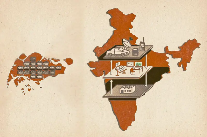
India, working from a continental platform with a 1,25,000 designers already inside its borders, has to play a different and harder game.
In 2024, a joint venture called VSMC - a Dutch-Taiwanese consortium formed by NXP Semiconductors of Eindhoven and a subsidiary of Taiwan's TSMC - broke ground on a twelve-inch wafer fabrication plant in Tampines, on the eastern side of Singapore island.
The fab will cost around $7.8 billion. It will produce chips at 40 and 55 nanometre nodes, the kind of mature-process silicon that runs the microcontrollers in car engines and the power-management parts in industrial robots. First wafers are scheduled for 2027. Full volume production in 2029.
This is the twenty-first semiconductor wafer fab currently operational or under construction in Singapore.
The island is 720 square kilometres - roughly half the size of Delhi proper. Its fab density is the highest of any jurisdiction on earth. Higher than Hsinchu in Taiwan. Higher than the clusters around Dresden in Germany or Malta in upstate New York. And no Singaporean company owns any of these fabs. Every one of them is operated by a foreign multinational: GlobalFoundries out of the United States and Abu Dhabi, Micron out of Boise, STMicroelectronics out of Geneva, United Microelectronics out of Hsinchu, TSMC through two separate joint ventures, Soitec from France, Infineon from Germany.
The wafers are made in Singapore. The companies making them are based elsewhere.
This fact - twenty fabs, zero domestic owners - is the Singapore semiconductor story in compressed form.
How it came to be that way, what it produces, what it is worth, and what it tells a country five thousand kilometres to the west which is now trying to build its own fabrication base, is the question this piece opens.
Singapore hosts over twenty semiconductor fabs on its 720 sq km island - every single one owned by a foreign multinational, from GlobalFoundries to Micron to TSMC.The Indian semiconductor push, formalised in December 2021 as the India Semiconductor Mission with a ten-billion-dollar budget that has since been enlarged, is often described by officials and commentators as following the "Singapore model."
The phrase is a short-hand and a misleading one.
What Singapore built was narrower than the phrase suggests. The Singapore project was to create a semiconductor host - a piece of real estate, infrastructure, and trained labour so well-prepared that foreign chipmakers would find it cheaper to manufacture there than anywhere else on earth.
This is a legitimate and lucrative strategy for a city-state with five million people and no domestic electronics market of consequence.
It is the wrong strategy for India, and the first thing an Indian policymaker should notice when looking at Singapore is how different the two bets are.
India can and should emulate parts of what Singapore did. The patience. The professional investment promotion. The dedicated wafer fab parks. The multi-decade horizon.
What India must not emulate is Singapore's ambition ceiling.
Singapore's ceiling was to be a manufacturing location on someone else's supply chain. India, if it plays its endowment right, has no reason to settle for that.
On 13 March 2024, Prime Minister Narendra Modi laid the foundation stone for India's first twelve-inch semiconductor wafer fabrication facility, at Dholera in Gujarat.
The fab is a joint venture between Tata Electronics and Taiwan's Powerchip Semiconductor Manufacturing Corporation. Total investment: approximately ₹91,000 crore, around eleven billion dollars. Nodes: 28, 40, 55, 65 and 90 nanometres - the mature end of the technology range, the same band in which Singapore's fabs now operate. Planned capacity: fifty thousand wafers per month. First chip out the door: late 2026 per the official schedule, though the industry consensus is that 2027 is more realistic.
The Indian taxpayer is paying for roughly half of this through central and state subsidies. Three other chip assembly and test plants - in Gujarat and Assam, backed by Tata, Micron, Kaynes Technology, CG Power-Renesas, and HCL-Foxconn - are in various stages of construction, together absorbing another few billion dollars of subsidy.
This is what India has committed to. The question of whether the commitment will produce a semiconductor industry or merely a semiconductor factory is a separate question.
Singapore answered it one way. India has not yet decided how it wants to answer.
The gulf between Singapore and India is not just geographic - it spans population, design talent, domestic market size, and strategic ambition, making the 'Singapore model' a misleading template for India.The Singapore story begins in 1968.
The country was three years old as an independent state, expelled from Malaysia, sitting at the southern tip of a peninsula with no natural resources and an unemployment rate near fourteen per cent.
Lee Kuan Yew's government had a Finance Minister, Goh Keng Swee, who believed the only way out was to attract foreign manufacturing - any foreign manufacturing - and turn the workforce into something worth employing.
The Economic Development Board, then six years old, was given the job of going out into the world and finding multinationals willing to commit.
In 1968 the EDB landed its first semiconductor customer: National Semiconductor Corporation of Santa Clara, California, which set up a transistor assembly plant in Kallang.
The work was low-skill by later standards - bonding wires to silicon dies under microscopes - and the workers were almost entirely women, recruited and trained in batches of fifty at the state's expense.
Texas Instruments followed in 1969. Hewlett-Packard in 1970. Fairchild, Motorola and Intel arrived through the 1970s.
By 1980, semiconductor assembly in Singapore employed more than thirty thousand people, almost entirely in the back-end of the industry - packaging chips made in American fabs, testing them, and shipping them on to Japanese and European customers.
Singapore had cheap, disciplined, English-speaking labour and a government that worked. Fabrication was what the country lacked. The wafers still came from Santa Clara or Phoenix or Austin. Singapore was the finishing station. This was the first rung.
The second rung required capital the private sector would not commit. Wafer fabrication in the 1980s was a multi-hundred-million-dollar bet per factory, with process technology evolving every two years and capital equipment written down over five. No Singaporean private firm had the balance sheet or the appetite. The state did.
In 1987 the government, through Temasek Holdings, incorporated Chartered Semiconductor Manufacturing. The company was capitalised with hundreds of millions of dollars of public money, given a plot of land at Ang Mo Kio, and told to learn how to run a fab.
The core technology was licensed from Sierra Semiconductor in California. The managers were recruited from the American majors, many of them returning Singaporeans who had gone abroad for graduate degrees in the previous decade. The first wafers came out at 2.5 micron - which is to say, at a process node that was already two generations behind what Intel and TSMC were running when Chartered opened. Catching up was the point.
By 1994 Chartered was at 0.8 micron. By 1999 it was at 0.25 micron and had just listed on NASDAQ, a Singapore Inc. IPO that the island's financial establishment treated as a coming-out party for its industrial economy.
Chartered never quite caught the leading edge - it was always a generation or two behind TSMC, Samsung and Intel - but it had demonstrated something that had never been demonstrated before: that a small Asian state with no domestic semiconductor demand could run a competitive pure-play foundry.
For a while in the 1990s, Chartered was the third-largest foundry in the world.
What made Chartered possible, and what made the broader Singapore strategy possible, was a man named Philip Yeo.
Yeo ran the EDB from 1986 to 2001 and afterwards chaired A*STAR, the country's main public research agency.
He was an engineer by training, a civil servant by vocation, and a closer by temperament. His method was to go to the American majors, find the engineering vice-president who was frustrated with his current manufacturing location, and offer him everything he asked for - land, power, water, tax breaks, custom-built facilities, staff recruited and trained at state expense - in exchange for a firm commitment to put a fab in Singapore.
He would then see the deal through to groundbreaking personally. Much of Singapore's current semiconductor footprint traces back to one of Yeo's handshakes. A generation of Singaporean civil servants grew up inside that operating culture, and the culture persisted after Yeo left the EDB.
The 1990s were Singapore's fab decade. STMicroelectronics opened an eight-inch wafer plant in 1994. TSMC, Philips (which later became NXP), and the Singapore government jointly built SSMC - Systems on Silicon Manufacturing Company - in Pasir Ris, coming online around 2000. It is still operating, now majority-owned by TSMC, and it is one of the reasons Singapore can legitimately claim a TSMC fab on its soil even though TSMC's flagship operations remain in Taiwan.
UMC of Taiwan built its own Singapore fab, UMCi, starting in 2000. Applied Materials, ASM and Lam Research - the three largest semiconductor equipment makers in the world - established regional operations in Singapore, many of them with manufacturing attached.
Micron entered the country in the late 1990s with an assembly plant and later, crucially, chose Singapore as its principal site for memory wafer fabrication outside Idaho and Taiwan.
By the mid-2000s, about a tenth of the world's semiconductor output by value was being manufactured somewhere in Singapore - a share that has held roughly steady in the two decades since.
From a transistor assembly shop in Kallang in 1968 to the world's densest fab cluster six decades later - Singapore's semiconductor journey in nine milestones.And then, in 2009, came the moment that revealed what the Singapore strategy actually was.
Chartered, the national champion, had been losing money for most of the 2000s. The foundry business is brutal at sub-scale, and Chartered had never reached the scale of TSMC or the capital depth of Samsung.
In September 2009, ATIC - the Advanced Technology Investment Company, sovereign wealth fund of Abu Dhabi - announced it would buy Chartered for close to four billion dollars all-in and merge it into GlobalFoundries, the newly formed foundry spinoff of AMD.
Temasek sold. The deal closed in January 2010. Chartered Semiconductor Manufacturing, after twenty-three years as Singapore's flagship chipmaker, ceased to be Singaporean.
In Singapore the sale was not treated as a defeat. The country got back a cheque measured in the billions, kept the fab, kept the jobs, kept the workforce, and gained a GlobalFoundries Singapore that was part of a larger global foundry network with more scale and more R&D depth than Chartered alone would ever have mustered.
From the strategic point of view of the Singapore state, the sale made Chartered a more viable fab by removing the burden of being a standalone national champion. The fab continued. The firm went away.
This was the revelation. The destination Singapore had been walking towards all along was a host economy - a dense cluster of foreign fabs on Singaporean soil, with the country collecting the rents, the jobs and the skills transfer.
The sovereign firm had been a route, and the route had been completed.
The Chartered sale made the destination explicit. From 2010 onwards, Singapore's semiconductor policy was wholly and openly a strategy of being the best manufacturing host on earth for firms owned and headquartered elsewhere.
The country stopped trying to have its own TSMC and committed fully to being the place where other people's TSMCs did their work.
In the fifteen years since, the strategy has paid off.
GlobalFoundries has announced a $4 billion expansion of its Woodlands campus, adding 300,000 wafers per year of capacity.
Micron has put in more than seven billion dollars in successive waves of DRAM and high-bandwidth-memory investment, the most recent wave directly targeting the AI accelerator market that has redrawn the memory business.
UMC is building a new twelve-inch fab in Pasir Ris.
VSMC - the NXP, TSMC and Vanguard joint venture that opened this piece - is under construction in Tampines.
STMicroelectronics runs a large plant in Ang Mo Kio.
Soitec, the French silicon-on-insulator wafer specialist, chose Singapore for its Asian manufacturing.
Infineon does back-end and some design here.
Between them, these companies and about a dozen smaller ones employ around thirty-five thousand people directly in semiconductor manufacturing, and support perhaps twice that indirectly through equipment, specialty chemicals, logistics and services.
Semiconductor manufacturing accounts for around six to seven per cent of Singapore's GDP, and sits at the heart of a wider electronics cluster that is larger again.
What Singapore actually produces is worth being precise about, because the precision matters for how India should read the story.
Singapore does not fabricate leading-edge logic. The 3-nanometre, 5-nanometre and 7-nanometre processors that go into the most recent iPhones and NVIDIA accelerators are made somewhere else: Taiwan, South Korea, and increasingly Arizona and Kumamoto where the most advanced new fabs are under construction.
The most advanced node in volume production on Singapore soil today is around 22 or 28 nanometres, at GlobalFoundries. Most of what Singapore makes is further back again - 40nm, 55nm, 65nm, 90nm, 130nm, 180nm - the so-called mature and specialty process nodes.
These nodes are unglamorous. They are also enormous. The world's cars, power systems, industrial sensors, medical devices, consumer white goods, and much of its defence electronics all run on mature-node silicon.
Prices per wafer are lower than at the leading edge, but volumes are higher, the equipment is paid off, and the processes are mature enough to be tuned for automotive and industrial qualification.
The business is profitable precisely because it sits off the leading edge, where margins are crushed by the capex cycle. Singapore also runs significant memory fabrication - Micron's DRAM and NAND plants, including the island's most advanced memory capacity outside Taiwan and Korea - and significant back-end assembly, packaging and test.
The assembly work is lower-value per employee than fab work, but it is where a great deal of the employment sits. And the country is one of the world's largest suppliers of semiconductor manufacturing equipment too, through Applied Materials Singapore, Lam Research Singapore and others, which underwrites Singapore's frequently cited claim that it produces roughly one-fifth of the world's semiconductor equipment output by value.
What Singapore does very little of is design. The country has no globally significant fabless semiconductor company of its own. Broadcom, which is legally headquartered in Singapore for tax purposes, was an American design house before the move and remains American in every substantive sense - its engineering is mostly in California and Pennsylvania; it pays its taxes in Singapore without building a design ecosystem there.
A*STAR's Institute of Microelectronics does serious research in specific niches - advanced packaging, MEMS, silicon photonics - while remaining a research institute rather than a commercial design base.
The large MNCs have some design teams in Singapore, but none at the scale of their Indian or Chinese or Israeli design centres. The country has roughly two to three thousand semiconductor design engineers, depending on how one counts. The equivalent number in Bengaluru alone is somewhere between eighty thousand and a hundred and twenty thousand.
The absence of design follows from the strategy rather than running against it. Chip design is a people business - it scales with engineering headcount, requires dense local talent networks, rewards access to large and varied consumer markets from which design insights flow. Singapore's population is not big enough to feed a world-scale fabless firm, the country is expensive for the kind of mid-career engineering talent that fabless companies run on, and the end-market insights a fabless company needs - what chips the customer wants next year - flow better out of large domestic electronics industries than out of city-state economies.
The Singapore state did these sums in the 1980s and concluded that fabrication was where its comparative advantage lay. It has stuck to the conclusion for forty years.
The strongest argument in the opposite direction deserves stating in its strongest form, because it is the argument most sophisticated observers of the semiconductor industry would make.
The argument begins with a simple observation. Of the countries that have actually built successful semiconductor economies in the last forty years, hardly any did it through the sovereign-firm route.
The Netherlands dominates lithography through ASML, which is the world's only maker of extreme-ultraviolet machines, yet the Netherlands has no significant chip designer of its own.
Taiwan is the world's foundry, but TSMC is a foundry - it makes other people's chips - and Taiwan's fabless design sector, while real, is a modest tail on a very large fab dog.
South Korea has Samsung and SK Hynix, but both are primarily manufacturers with in-house memory design, and neither has produced the broad design ecosystem the United States has.
Even the United States, the only country that possesses a complete semiconductor stack, is hollowing out its manufacturing layer - most American-designed chips are now fabricated in Taiwan or Korea, and the American design industry, world-class as it is, depends on Asian manufacturing to function at all.
The pattern this suggests is that semiconductor value is captured through manufacturing, equipment, materials, and specialty process technology - not, for most countries, through fabless design.
A country that owns a few good fabs, a dependable place in global supply chains, and an integration into the equipment ecosystem can capture a very large slice of the industry's economic output even without owning a single major fabless firm.
Singapore is a textbook case of this argument. It has no Qualcomm, no NVIDIA, no MediaTek, no Broadcom-of-its-own, and yet it captures something in the order of a hundred billion US dollars of annual semiconductor-adjacent economic activity.
The "Singapore has no industry" framing is wrong on this reading. Singapore has a very large industry; it just happens to be the manufacturing and equipment part, which is the profitable part.
Applied to India, the argument becomes: do not waste energy trying to build Indian fabless champions, which will take decades and may never match the American and Taiwanese incumbents. Build fabs and attract foreign fabs, as India is now doing. Let the design work continue to be done by the 125,000 Indian engineers currently employed by foreign semiconductor firms in Bengaluru and Hyderabad. Let the fabrication gradually grow. Over a generation, accumulate the kind of cluster Singapore has taken sixty years to build.
This is the Singapore template. It has worked once. It can work again.
The counter-case is serious and parts of it are correct. The implication drawn from it - that India should go host-first and leave sovereignty for later, or leave it alone - is wrong, and the reason has to do with scale.
Singapore is five million people on 720 square kilometres. Its domestic electronics market is a rounding error on a global scale. Its total labour force tops out at around three and a half million. It cannot, even in principle, support a Qualcomm or a MediaTek - the engineering headcount alone would absorb something like a third of the country's workforce. Singapore's embrace of host-country status was an embrace of its own scale ceiling. For a city-state there was no other game to play.
India is not a city-state. Its domestic electronics market is projected to cross four hundred billion dollars by 2030, of which perhaps a sixth to a quarter will be chip-content by value - the Indian internal market for silicon is already larger than the total semiconductor output of most of the world's national industries.
India has 125,000 to 150,000 active semiconductor design engineers, comparable to Taiwan's total and a meaningful fraction of America's.
It has defence, space, and telecommunications use cases that will continue to demand sovereign supply irrespective of what global markets do - the ISRO cadence alone requires a secure indigenous path for space-grade silicon, and the armed forces' appetite for autonomous munitions, radar systems and encrypted communications will not be satisfied by foreign fabs under any likely geopolitical configuration of the next twenty years.
India has, in short, all the endowments that Singapore did not have: a large internal market, a deep and cheap talent bench, irreducible sovereign demand, and a strategic environment that penalises dependency.
To be India and run the Singapore game would be to decline these endowments.
It would be to run the city-state playbook from a continent-sized platform.
The Tata-PSMC fab in Dholera, on its own, will produce chips. Whether those chips are made for Indian designers, by Indian designers, in pursuit of Indian product ambitions, is a separate question.
The Singapore model answers that question in the negative - the chips are made, and the country does not greatly care whom for. India has the option to answer it in the affirmative, and its current industrial design has not yet chosen which answer it wants.
What would owning the stack look like? It would look, in outline, like what Taiwan did across the 1980s and 1990s and what Korea did from the 1970s through the 1990s, compressed into a shorter timeline because India has the late-comer's advantage: the fabs, the design tools, the IP libraries and the equipment supply chains all exist now and can be purchased rather than invented from scratch.
The pattern is familiar. A domestic fabless company designs a system-on-chip for an Indian end-product - a smartphone, a base station, a car, a defence radio, a satellite payload. The chip is fabricated at an Indian foundry. The end-product is built by an Indian OEM and sold into Indian and export markets. Every link in that chain exists in India today in some form. What is still missing is the coordination that connects one link to the next.
The coordination problem is substantively harder than the fabrication problem, which is one reason the fabrication problem is getting the larger share of attention.
Fabrication is solved by writing cheques to firms with proven technology and supervising construction. Coordination is harder: it requires aligning the procurement priorities of several ministries, the design risk appetite of a dozen private Indian OEMs, the investment horizon of venture capital, the skills-to-project matching of a supply chain still being assembled, and the production schedule of a foundry still being built.
No country has solved the coordination problem on a fast timeline without a heavy guiding hand from the state, and the hand has to guide in a particular way - as anchor customer taking the first production units, specifying the requirements, absorbing the early yield losses, giving the private supply chain the visibility and volume commitments that make each next round of private investment rational.
The Taiwanese state played this role through ITRI, the industrial research institute that incubated TSMC and UMC and eventually moved both into the private sector with a book of orders attached.
The Korean state played it through the chaebol structure and an industrial policy willing to guarantee demand for what Samsung and Hyundai decided to build. Both states were buyers first and subsidisers second.
India's version of this - the Indian version, fitted to Indian federal structure and Indian procurement culture - is the work the next phase needs. Some of the shape will be obvious once the effort is organised.
Defence and space are the natural starting point, because the sovereign buyer is already in place and the requirements are concrete: specified chip classes for next-generation radar, for encrypted communications, for space-grade redundant systems, for guided munitions and loitering ammunition, matched to specified Indian fabless firms and specified Indian fab capacity, with procurement commitments that run on ten-year horizons rather than annual ones.
A Defence Semiconductor Roadmap of that shape, published and binding, would do more for the fabless-champion question than another round of fab subsidy.
Telecommunications is the adjacent frontier: Indian operators deploy more 4G and 5G base stations per year than American operators do, and none of those base stations currently uses Indian silicon.
A graduated local-content rule for Indian telecom networks, paired with capital support for the Indian firms that would supply the chips, would create an anchor market at commercial scale.
Automotive sits on a ten-year horizon as Indian car makers move into electric platforms where chip content per vehicle is larger and the specification can increasingly be set at home.
Each of these is a place where the state is already, or could easily become, the anchor customer. Each is a place where Indian firms with Indian IP can be pointed at Indian demand.
Four sectors where the Indian state can act as the anchor buyer to underwrite sovereign semiconductor supply - from immediate defence and space needs to the ten-year automotive horizon.None of this replaces what India has already started to build. The Tata-PSMC fab at Dholera, the Micron assembly plant at Sanand, the Tata and Kaynes and CG Power facilities for assembly, test and packaging - these are the base of the stack, and without the base nothing else is possible. They are necessary.
The argument is that they are necessary and the beginning, and that the layers above them - fabless champions, anchor demand, integrated end-products - are the layers the next phase has to build.
India's semiconductor industry has its base layers under construction - wafer fabrication and assembly. The harder layers above - fabless design champions, anchor demand, and integrated end-products - are what the next phase must build.India is not a rentier state, and the Singapore playbook is a rentier's playbook.
A country with a continental market, a hundred and twenty-five thousand semiconductor designers already at work inside its borders, and a defence-space-telecoms demand profile that will not be satisfied by imports under any plausible geopolitical future has a harder road in front of it than Singapore ever walked.
The road is harder because owning the stack is harder than renting the geography.
It is also the road the endowment points towards. To decline it would be to run someone else's strategy on a platform built for a different one.
When the VSMC fab in Tampines begins production sometime in 2029, the chips coming off its lines will be 40-nanometre and 55-nanometre automotive microcontrollers and industrial power-management parts - unglamorous silicon in very high demand because it underpins the electrification of everything.
Those chips will have been designed by engineers in Eindhoven and Hsinchu. They will be sold into the cars, factories, and appliances of every major market on earth.
Singapore's role in this chain is to be the place where the wafers happened to get fabbed. The wafers could theoretically have been fabbed elsewhere; they are fabbed in Tampines because Singapore spent sixty years making sure Tampines was the cheapest and safest place on earth to fab them.
Every stage of that sixty-year effort was a state investment in a particular ceiling. Singapore has reached the ceiling, and the country is rightly proud of having climbed to it.
India's Dholera fab, when it opens in 2027 or 2028, will produce chips at similar nodes for similar customers. The immediate economic picture will look a great deal like Singapore circa 2005. What will differ, over the ten and twenty and thirty years that follow the first silicon, is whether an Indian design and electronics industry grows up around the fab.
Singapore did not attempt that second thing because it had no reason to - the endowment that would have made it possible was absent. India has the endowment, and the second thing is the whole point of the first.
The twenty fabs on a 720-square-kilometre island are the picture of a rentier strategy played beautifully by a country that knew its own ceiling. India's platform is continental. Its answer has to be ownership - Indian companies designing the chips, owning the IP, feeding Indian foundries, building the end-products, and closing the loop that today runs broken in several places.
In the first phase of that work the state has to act as the buyer who underwrites the beginning, through defence procurement, through telecom local-content rules, through the long-horizon commitments that let Indian firms raise capital and compete against global incumbents.
In the second phase the market takes over. The generation now being trained in VLSI design at the country's engineering colleges is the generation that will build the loop, and the country they build it in will be richer, more sovereign, and more present in the world's electronics than the most successful rentier could ever be.
That is the argument for the harder road. The Singapore story, read carefully, is the argument for taking it.